
The front panel is dominated by the large dot-matrix LCD, for displaying the levels of all the inputs and outputs, analog and digital, as well as the current clock frequency and source. The other half contains the gain adjust encoders for the analog inputs, as well as pads and phantom-power switches per channel, and the headphone output with associated volume control.

A neat layout on the back as well. A nice touch - Amphenol connectors (as opposed to some far-easter no-name) for the analog inputs, all eight being "combo" sockets. Eight 1/4" jack sockets carry the analog outputs, and then there's all the digital I/O: two banks of ADAT Lightpipe (for up to 16 ins & outs), Thunderbolt, USB 2.0, and this unit's party-piece, an AVB connection. Oh, and Wordclock BNC in & out.
This time around, i did indeed go against the foremost commandment of teardowns, and powered up and tested the unit out, before popping the top off. It cost me a pretty penny, i bought it as working, and i wanted to make sure i got my money's worth! But that was an ever so slightly bumpy ride - the latest driver version i had already downloaded, required firmware version 1.2.7 (which i only noticed after a couple reboots, and then reading through the driver release notes). The unit turned out to still be running the factory firmware, version 1.0.0. Updating that went smoothly enough, and a couple minutes it was all up and running.

Back to the task at hand, then. Not a whole lot of room to spare in here, they crammed in just about all they could fit in here, without ending up with too ratsnest-y of a layout. But let's take a look in slightly more detail then, shall we?

Right off the bat, my view was captured by a couple small... design boo-boos. The power supply used here is an age-old design, one i first encountered in a later-revision 8Pre, as well as in the "mk3" range of interfaces. In those, the processing part was on the same board as the rest of the circuitry, so the only connection board needed was a tiny one, just enough for the two sockets. This time around though, in addition to needing to pass power to both the processor board and the analog I/O board, they also needed a good few data lines between the latter two. But they perhaps couldn't be bothered to source some shorter 0.1" sockets for the PSU connection? Or some of those through-board ones? Either way, this board is nowhere near level due to the 2mm-pitch sockets on the left side are much less tall than the 0.1" / 2.54mm ones on the PSU side.

Design vs. manufacture issue no.2 - how to fasten both the LCD and the user interface board to the front panel. I'll have to figure out some more definite solution there, because the channel 7-8 buttons have an extra 0.5-1mm of (mushy) travel before the tactile switches actually click, and that's... unacceptable. It doesn't really help that there's a height (or thickness) difference between the LCD PCB and the UI one. But that's not really such a major issue, barely beyond "cosmetic".

Right then, let's get right into the thick of it, starting off with, as usual(?), the power supply. As expected, precisely the same model as in their older units - see the "Copyright 2006" silkscreened on the board, near the bottom of the big electrolytic? OEM seems to be [ahem] "Hon-Kwang" - a sonorous by-word for longevity and reliability, right? Well, an 828mk3 i bought, fixed and flipped a couple years back would somewhat disagree - the big 400V electrolytic leaked its guts and corroded one of the traces, so the thing didn't power up at all. Needless to say, this'll be the first thing to get re-capped, ASAP.

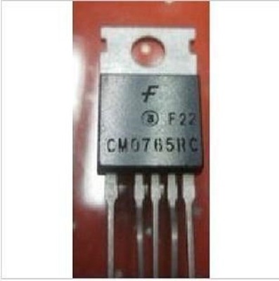
Primary-side electrolytic is a 33uF 400V JunFu - yummyyyy... Secondary has a couple tall Teapo SC's, and a couple SWC-brand ones. Feel free to shudder. The PWM controller is an all-in-one job, an FSCM0765R. The original seems to have been made by Fairchild Semiconductor, but this must be some second-source one - no italic "F" logo or anything. Secondary-side rectifiers are four SR5100 5A 100V Schottkys and there's a SOT-223-packaged TPS79633 linear regulator for the 3.3V rail.

On to (some of) the "big guns" - here we have the main processor board. Unlikely to have any less than 4 layers, i'd reckon, what with the two "plentiful" BGA chips there. Smack-dab in the middle is a Texas Instruments OMAPL138B "C6-Integra DSP+ARM" processor. I'll let you browse through the 284(!!!) page datasheet at your own leisure, to get all the details and features of it. Assisting it are a Micron MT46H32M16LFBF-6 512Mbit / 64Mbyte LPDDR RAM chip, and a Spansion (now Cypress) S25FL256SAIF 256Mbit / 32Mbyte SPI flash ROM holding the firmware.
Quite cute that they silkscreened the "main role" of the traces coming out of each side of the chip: "DRAM" for the memory bus, "RMII" for the LAN side, "SPI1" for serial comms, "MCASP" for what turned out to be the audio I/O interface, and last but by no means least, "UPP etc".

Slightly "north" of it lies a Xilinx Spartan-6 XC6SLX25T FPGA. Oddly enough, it seemed to have a drop of some sort of oil(?) on it, hence the darkened markings. Regardless, given its feature set, at least one definite role it has, is PCI-Express communication with the Thunderbolt interface.


In the (nearly) "miscellaneous silicon" section, there are two Texas Instruments TPS4218's, in charge of the 1.2V (for the FPGA) and the 1.8V rails (for the OMAP processor), respectively.

On the back side of the processor board, only three silicon devices reside. Most noticeable of those is the Marvell 88E1116R Gigabit LAN transceiver. Second largest is the SMSC (now Microchip) USB3340 USB transceiver. The smallest chip near the "bottom" edge of the board is a Cirrus Logic CS2100-OTP clock multiplier / PLL.

You may or may not have noticed that the optical connectors on the back seemed sort of wonky - my first thought was that a couple of them maybe got dislodged during the wave-soldering stage, but then i noticed the faceplates were in fact level. Turns out they just used (most likely) optical transmitters from a different range (and/or manufacturer) than the receivers, hence the "inconsistent" footprint.

Moving on to the Thunderbolt daughterboard - arguably nice touch there, no doubt to lower the risk of failure, and/or allowing for separate troubleshooting of this section. If not even, who knows, ease of later upgradeability, but that may well just be wishful thinking.
Only two (relatively) big pieces of silicon on the top side - an NXP LPC1114 ARM Cortex-M0 microcontroller, and an Intel DSL2210 Thunderbolt controller. Powering those are a Texas Instruments TPS73033 RF linear regulator ("PHUI" marking), a TPS73533 linear regulator, as well as a Micrel (now Microchip) MIC47100 regulator.


And now, for the "main event" - the audio board. And a big and plentiful one it is, indeed.

Might as well start off with the most obvious(?) thing on the board, a Xilinx Spartan-3A XC3S400A FPGA. My best guess would be that this is in charge of marshalling the audio data to and from the converters, as well as the front panel (encoders / buttons / LCD) and driving the pad and phantom-power relays. It's surrounded by a Texas Instruments SN74AHCT245 bus transceiver (driving the LCD); a TI TLV1117 3.3V linear regulator; a TI PCF8574A I2C port expander; and a TI PCA9306 I2C voltage-level translator.

On the other side of the JTAG(?) header, we find a pair of TI TPS79650 linear regulators (most likely powering the converters, as well as the preamps - spoiler alert).

And speaking of which - no major surprise to see the venerable(?) TI PGA2500 digitally-controlled microphone preamplifiers in use here. If you're having some sort of feeling of deja-vu, it's well justified. We've seen these before in the MOTU Traveler Mk3, as well as the Apogee Ensemble. The line / instrument inputs seem to be buffered by a Rohm BA4580R on each channel. Two Omron G6J-Y relays per channel handle the switching of the attenuator pads and the phantom-power respectively. The SOT23-6-packaged parts seem to be OnSemi NDC7001C dual MOSFETs (N-channel/P-channel) - there's a good chance these might be driving the coils of the relays. Just as in the 828 mk2, we again see some monolithic bridge rectifiers used as input clamps. Interesting package that i haven't encountered before, but i've yet to manage to identify the exact part number.

Pictured here is one of the two Cirrus Logic CS5368 8-channel A/D converters. Since there are two of them, but only eight analog inputs, i've got a hunch this may well be where the (selectable) polarity-reversal of the signal is performed. The inputs to these are buffered and filtered by a pair of ST Microelectronics TS922 for each channel. The ninth (visible) TS922 off to the left buffers the mid-supply bias voltage from the ADC (Vq, hence the "VQ 1" and "VQ 2" silkscreening around it) and supplies that to the associated input filter opamps.

Slightly off to the side is the headphone output, with its own dedicated DAC, a Cirrus Logic CS4351. This then goes into an NJM4556A, which drives the physical output.

Off in the corner of the board there's some power supply-ing going on: a National Semiconductor LM2990S -5V linear regulator, providing the negative rail for the microphone preamps, and two TI TPS61081 boost-converters, complete with voltage-multipliers on the output, to provide the phantom-power (most likely one per four mic inputs), despite the 27V max output the chips are rated for.

Over on the output side of things, an ESS ES9018 "Sabre32 Reference 32-bit Audio DAC" handles the digital-to-analog conversion, while eight National Semiconductor LME49724 fully-differential opamps drive the analog outputs.

In the vicinity dwell two little linear regulators, both TI TPS73001's - one providing a 1.2V rail to the DAC, and the other feeding the Spartan-3A FPGA with another 1.2V rail.
And that about covers it - quite "some" amount of stuff to go through... Sadly, i don't have any 22uF (or larger) 63V SMD electrolytics in stock, so the full re-cap will have to wait another week or two. I'd kinda-sorta want to "do it right", and not half-ass it with glued-down through-hole electrolytics. I found some suitable and reasonably cheap Nichicon ones at Mouser, so i think i'll go with those. But i'll need to draw up a complete list, as long as i'm at it. In for a penny, in for a pound, right?
No comments:
Post a Comment