
... Except that recently, for whatever reason, it's been kinda flaky, and ended up giving up altogether. To aid with stability, i had also performed some hardware mods on the power supply side of things (as well as on the iPod's mainboard). The rationale behind that, at least in part, was the source of the above-mentioned mods, so i'll need to transplant those to this newer one as well.

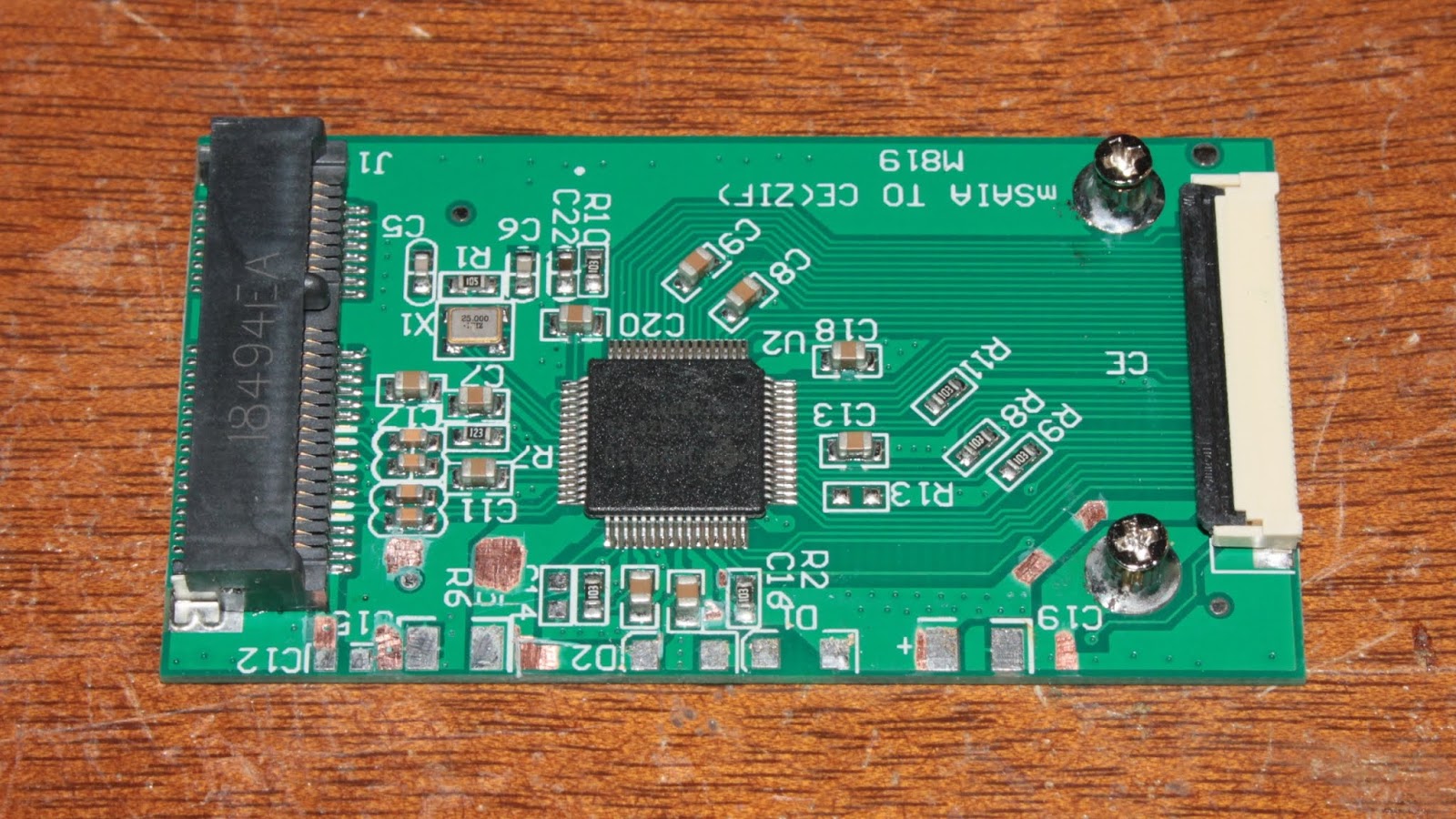
Not a lot of rocket-science going on here, just a no-frills datasheet implementation of the JMicron JM20330 "Serial ATA bridge chip". Well, except for the downright attrocious way to derive the 1.8V rail for the core supply - two series diodes coming off the 3.3V. I've heard of "cutting corners", but wow... Heeey, wait a minute - this new one's an "mSAIA" adapter - i want my money back!

The old one looks kinda like this. Yes, i know, a mutilated abortion of a thing, but in my defense, i didn't have much to work with, in the way of physical envelope. There's barely 2-2.5mm of space under the mSATA SSD when it's installed, and due to wanting to give this thing as much reserve-juice as i could, those fat tantalum-polymers on the 3.3v input wouldn't fit under there.

Also, if memory serves, at the time i might not have had any fixed 1.8V regulators for the core voltage (at least not in a package smaller than a DPAK), so i had to improvise a way to cobble together and shoehorn in an adjustable regulator, complete with the two setting resistors and the bypass capacitor. I'm in no way certain i've got any suitable regulators now, but one step at a time. In the hope of further "securing" this, i'll be adding a polyswitch and a 3.6V Zener on the 3.3V input as well. Better safe than sorry, or something-something...
I do very much appreciate the considerably sturdier ZIF connector on this new one, with the swing-down latch. The slide-latch on the old one is sort of iffy at best, and doesn't take much of a tug for the flex in it to slip out (even with the latch "on"). Also, i see they soldered the two threaded inserts (for affixing the mSATA drive) to their respecting groundplanes. Other than that, and the more detailed silkscreen (component designators etc), the two are virtually identical.

Right then, time to get the "list of ingredients" together. To start with, is scavenged two polyswitches (resettable fuses) off an old mainboard, one rated for 1.1A, the other for 2A. If things seem wonky with the first, i'll just chuck in the latter. Next, the Zener diode, a 500mW miniMELF recovered from a TV mainboard. And success - found a SOT-223-packaged 1.8V fixed regulator!
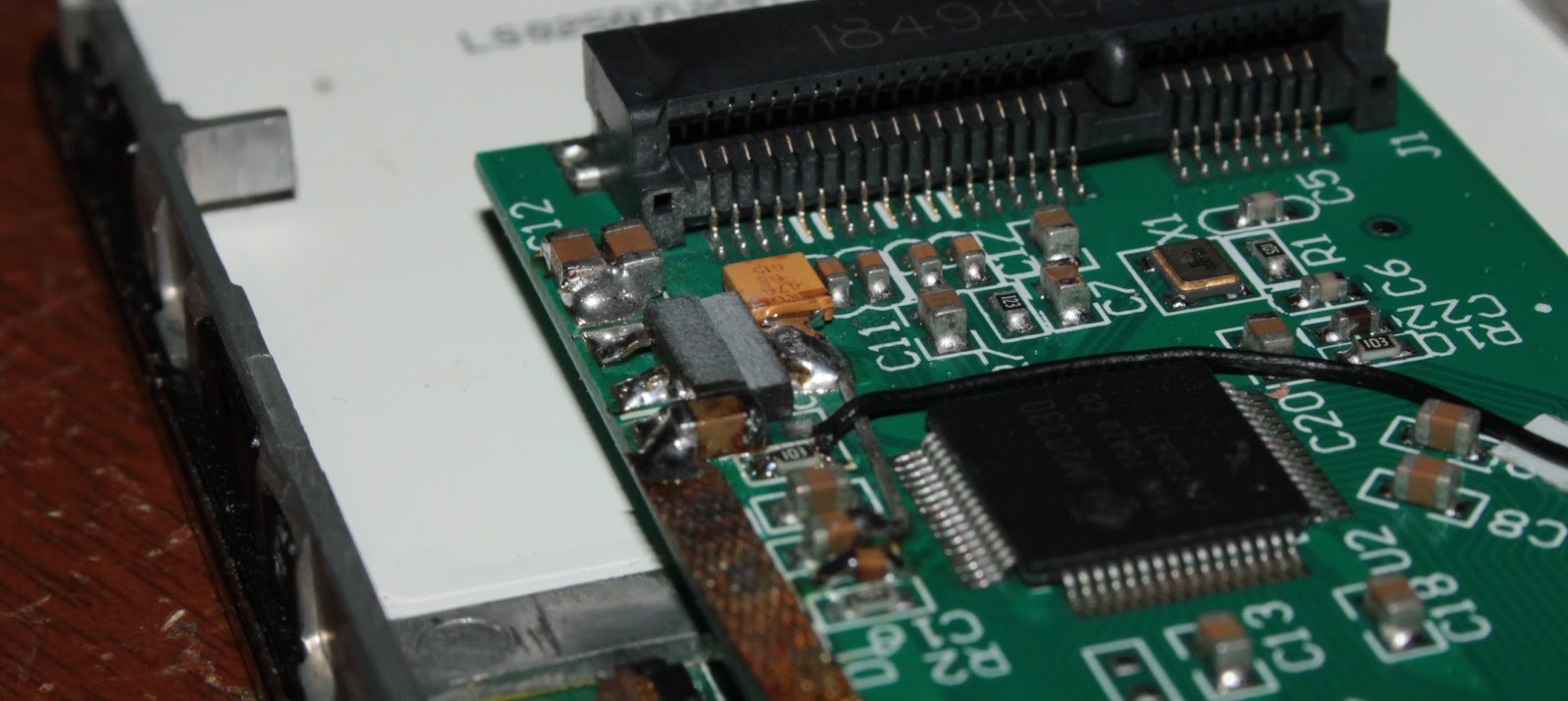
There, "extraneous" components cleared off and some soldermask removed to make new "solder pads". In the process, i also came across pin 44 (VCCO, 3.3V input/output power) with no bypass cap, so i took the liberty of clearing away some of the solder-resist to connect it between the 3.3V trace and ground (in between R2 and C16).

Theeeere we go, all soldered up. And the whole layout's a smidge more tidy than the first time around. I also moved the two bigger stock ceramic caps (one before and one after the two diodes) to the mSATA power bypass, right near one end of the connector - recycling and whatnot, right? And just for the hell of it, i reinforced the input 3.3V trace as well, with a bent-over resistor leg.
Quick test-fit aaaaand... Slight hitch. There's a wee chance that somehow, the mSATA slot might be ever so slightly lower than the old one. And/or this 1.8V regulator's a bit fatter than the adjustable one on the old board.
Ah well, needs must - out comes the file. Ended up "routing" a slot to make room for the edge of the controller chip on the mSATA drive to sit flush (as opposed to bending over / across the regulator as a pivot). You really do NOT want to subject BGA's to bending stresses. Well, unless you're in a "tempting fate" kind of mood, and/or you want to invite future problems.
On another whim, i went ahead and tacked on a drive activity indicator too. Well, partially also for potential troubleshooting purposes, down the line, just in case. That's driven by pin 34 of the JM20330 controller, designated "DASPn". Technically, in official nomenclature, the designation of the signal is "/DASP", the slash denoting that it's active low, but they probably wanted to avoid risking typos.
Due to the high brightness (or current efficiency, however you wish to call it), i went with a white LED scavenged from a broken laptop LCD. Even on my multimeter's 1mA diode-test range, it's plenty visible. Since the activity signal goes low during data transfers, one end of the "light emitter" (ie. LED with a current-limiting resistor in series) ties to the 3.3V line, and the other end to the signal pin.
3.3V minus the roughly 2.6V drop of the LED leaves us with 0.7V to drop across the series resistor. I wanted to go a little bit brighter than at 1mA, so for 2mA, the necessary value for the resistor is 0.7V divided by 0.002A, so 35 ohms. That's not a standard value, and on short notice i couldn't find any 33 ohm ones. On the TV board i scavenged that 3.6V Zener though, i found a few 75 ohm ones; a pair of those in parallel is 37.5 ohms, well within "ballpark".
... Buuuut something's still wonky - startup's quite unreliable. There's barely one quick blip on the drive activity LED (glad i tacked it on). To be fair, the controller's datasheet, on the last page, DOES mention that the 1.8V should come up either before the 3.3V rail, or worst case, at the same time. Given the setup, i have certain doubts that's happening, since the added regulator has to fill up all the capacitors on the 1.8V rail, and supply the chip, and that takes time. Right then, nothing left but to whip up some start-up delay circuit for the 3.3V rail.
The main idea here is to run a wire straight from the 3.3V input to the input of the 1.8V regulator, and then have the output of that "flip a switch" that then passes through the 3.3V to the rest of the board. Easiest way to do that is with a P-channel MOSFET as the switching element. After a bit of digging, i found a suitable candidate on a dead laptop board - an Si2315BDS, rated for 3.4A for a 2.5V gate drive. Plenty good for the purpose, and in a tiny SOT-23 footprint to boot.
But to get that to conduct, its gate needs to be pulled to a lower voltage than its source pin. Since our 1.8V is our "trigger signal", and is positive, all we need is a signal inverter of sorts - a so-called follower switch. Since we've only got such a small voltage to work with, that rules out most MOSFETs (since they need 2-4V applied to the gate, in order to start conducting), but we have NPN transistors, that need a measly 0.6V to conduct. Which leads us to this little setup:

I'll freely admit, much of the inspiration is taken from the power source switching (between DC input and battery) methods found in laptops. But hey, why reinvent the wheel, right?


I know, it looks like a rats' nest, but preliminary testing seems to indicate that did the trick - three out of three power-ups and shutdowns without a hitch.

Some problems did rear their ugly head(s) though. But after a couple evenings of fiddling about, i finally narrowed it down to the pesky little flex-ribbon cable between the drive and the mainboard. During maneuvering and drive-swapping and whatnot, the part that was supposed to be flat inside the latched ZIF connector on the mainboard managed to fold up a tad, but just enough for about half the pins to not make (reliable) contact with the pads on the end of the ribbon cable.
No comments:
Post a Comment