
Lots of ins & outs available on the back. Looks like it has some "smart TV" functionality as well, given the LAN port, as well as the USB socket marked "Wi-Fi".

I wonder if Sony's brand name for IEEE1394 / Firewire (ie. iLink) is no longer a trademark. Or is "Music iLink" different enough?

Either way, i can't really see any fasteners for the plastic top cover, so it's most likely clipped on. Oh joy... Fortunately, i managed to get a hold of the service manual, which includes disassembly instructions. Let's see how traumatic these end up being.

As it turns out, not at all - two screws and the top cover comes off. The HEAVY top cover, that is. Two observations here: on one hand, there's definitely a metal plate embedded in here, to give the whole thing a convincing weight, because the human being is a simple creature, and possibly so the whole thing doesn't rattle itself off of wherever it's sitting, when the DVD/BluRay starts spinning; on the other hand, i was wondering where and how i could even turn the thing on without a remote.

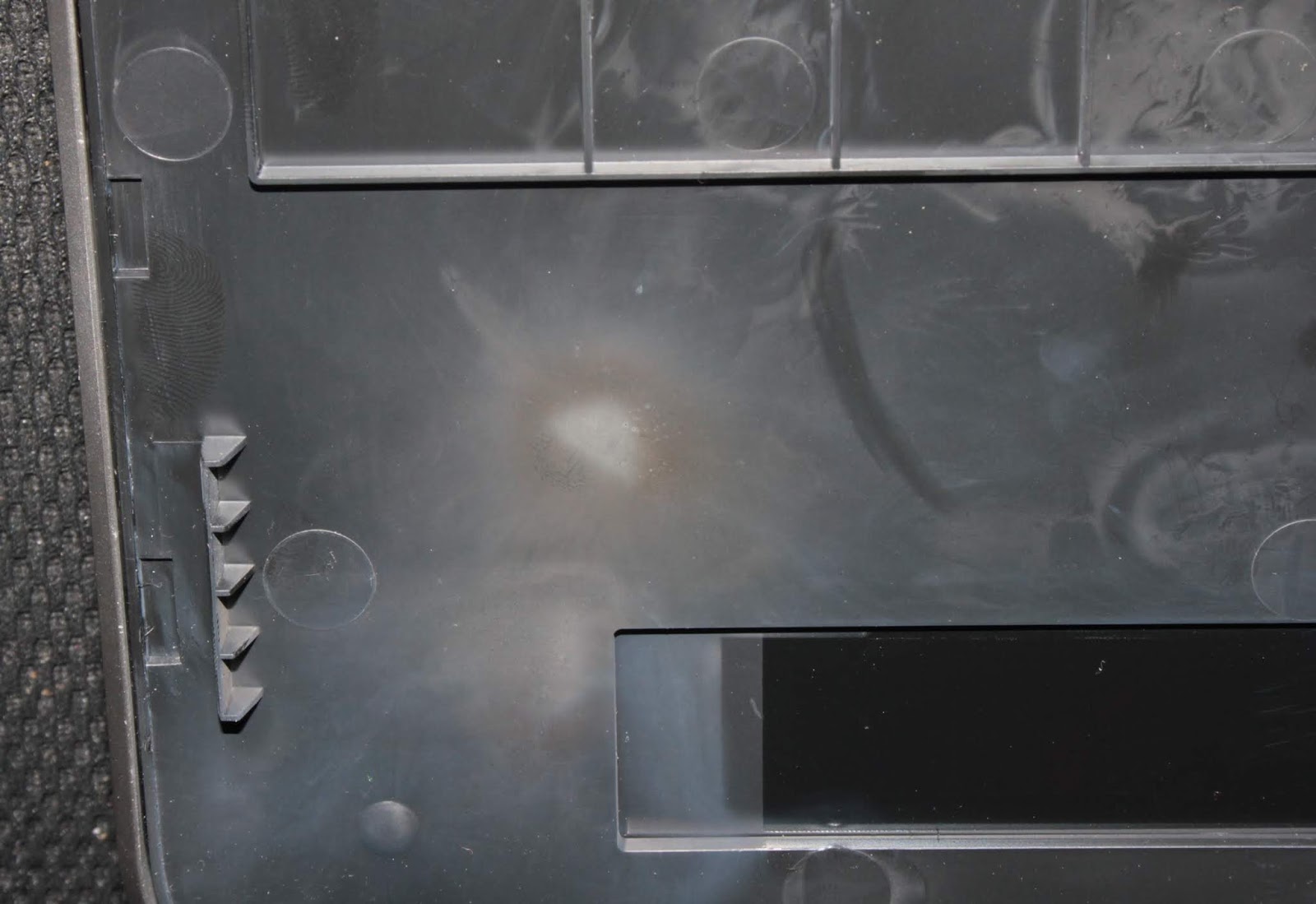
But on the underside of this top cover there's a window for a VFD, and a PCB carrying an Elan eKTF4701 controller (couldn't find any data on it), and what seem to be touch-sensors. As well as some "skidmarks"...

And here's an ensemble view of the innards. Since the skidmark on the top cover is near the VFD window, what do we find here? Oh lookie - the mains side of the power supply.

Here's a better view, to get an idea of the relative location of the source of the ejection of magic smoke. Sort of in the area of the two bulk filter caps (for the rectified mains input). But in-between them, there are also a couple of smaller heatshkrink-wrapped components. Since Y-class capacitors are not routinely "packaged" this way, these will most likely be metal-oxide varistors. With lots of "spikey" mains, these will eventually wear out (quite literally) and end up getting well-toasted (by way of failing short-circuit), hence the heatshrink "straightjacket", to contain the potential (or inevitable?) conflagration. One can even see patches of soot on the sleeving of the tall electrolytics, quite consistent with the direction of the end-opening of the heatshrink.

Given all this, the MOVs will obviously need replacing, and if those gave up the ghost in the manner that they did, odds are good that the fuse has gone bye-bye as well. But in the mean time, let's have a closer look at what's in here.
Interestingly enough, the front panel is actually made out of metal - possibly aluminium, but with an interesting paint-job (or perhaps just anodized with some nickel-looking colour after giving it the brushed finish).
"Lovely" capacitor brand choices for the power supply - Aishi and... Is that "Tbor"? You be the judge.


Out of the three transformers on this board, going by the two TO126-packaged transistors next to it, i'm gonna guess and say the smallest one is a gate-drive transformer for the two MOSFETs for the power amplifier supply rail - this involves the biggest transformer. The "medium" one puts out all the other voltages (12v and 5v for the optical drive, and whatever else is required), including the stand-by rail (since there's no power switch on the mains input).

Hunch confirmed - the lone DIP-packaged chip on the power supply secondary side is an Advanced Analog Circuits AZ7500BP - the part number most likely derived from FairchildSemi's KA7500, which itself is the equivalent of Texas Instruments' venerable TL494. The main power devices are a pair of Kodenshi AUK SMK1350F and one SMK0460F.

The bottom side of the board double-confirms it, with the traces from the gate-drive transformer going to the pair of MOSFETs then on to the big transformer.

A Sanken SSC620S PWM controller is in charge of the "small" power supply.
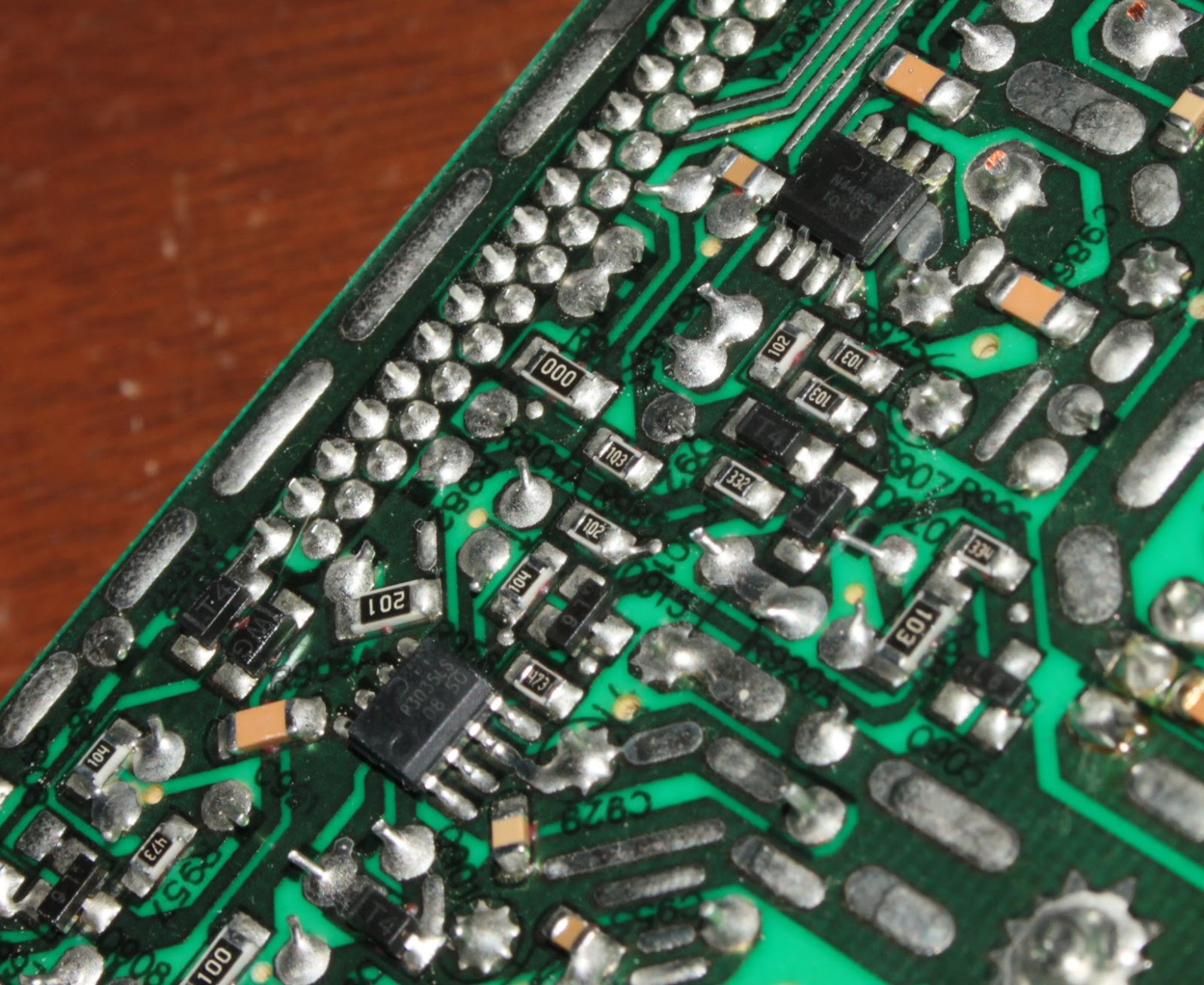
The only other notable SMD devices on the bottom of this board are two MOSFETs from Diodes Inc, a DMP3035LSS P-channel, and a DMN4468LSS N-channel. These two will be driven by whatever the stand-by supervising microcontroller is, to turn on the power to the "higher level" circuitry.

Audio board's turn. As one might expect, especially given the (relatively) slim form-factor and lack of humongous heatsinks, class-D amplification is involved. That being said, those are some considerably-sized inductors there. This being a 2.1-channel (stereo plus a subwoofer) unit, most likely there are two full-bridges for the stereo outs, and a parallel-bridge (PBTL) for the more current-hungry bass channel.

I'll hazard a guess and say this ST STM32F100 is always on and more or less running the whole show ("from behind the scenes", if you will). I'm basing that partially on the relatively low-frequency crystal right next to it. In the same area is a Cypress FM25C16B ferroelectric memory chip, containing the firmware - this might be the first time i've encountered one of these.

The analog inputs are digitized by a Cirrus Logic CS5346 stereo ADC, which includes a 6:1 multiplexer on the input.

In the middle of the board is a Cirrus Logic CS48540 audio DSP, in charge of decoding and processing the audio (Dolby, DTS etc, as well as downmixing 5.1 / 7.1 soundtracks to stereo).

Speaking of stereo, next in line is a Texas Instruments TAS5508C PWM processor. I didn't bother removing the board to be able to see what's under the heatsink, but the datasheet mentions the TAS5111, TAS5112 or TAS5182 H-bridge power stages, so odds are good that whoever designed this may not have strayed too far from those pointers. The first two are specified for an "absolute maximum" 33.5v supply rail, and while the silkscreen on the big fat power trace going to the amplifier says "+33V", that's cutting it a bit close (imho). But hey, if the amps didn't blow up or melt so far...

Over in the corner, a lone Artschip RC4558 dual opamp resides, possibly doing some buffering for the "Music iLink" input on the side (which is where the 3-pin stems from).

the 2SD882 transistor is most likely a discrete regulator providing the gate-drive voltage for the power stages. Next to it, pair of LD1117A's handle the 3.3v and 1.8v supplies for the digital circuitry on the audio board.

While we're at the "teardown" stage, out comes the "main" board. Not a while lot going on the back side, save for mostly passives, and a bit of power circuitry for the optical drive.

The heavy lifting is done by the heatsinked MediaTek MT8555 system-on-chip - i couldn't find any data on it. It's surrounded by four Hynix H5TQ1G63DFR DDR3 RAM chips, totalling 512MB. Nearby, a Hynix HY27UF082G2B 256MB flash ROM chip that holds the firmware, settings etc. To the left of that is an unpopulated footprint that looks remarkably like a SATA connector. Maybe it ended up cheaper to use a "bare" optical drive and do all the processing externally?

This is where the chips on the bottom of the board come into play. In addition to a Diodes Inc AP1117, the metal-topped one is a Renesas R2A30209SP. Couldn't find any data on this either, apart from some hints that it may or may not be a 6-channel motor driver. Makes sense, given that the spindle motor of the optical drive would need 2-3 outputs (being brushless), one for the sled the optical head rests on, and one for the tray (unless i'm forgetting something). The focus coil may or may not be driven from it too; my doubts stem from the much lower power and much finer control that would require, compared to the actual rotating electrical motors.

On the other side of the same corner of the board is a Texas Instruments TPIC1390CT(?) - must be some OEM-only part. Definitely has something to do with the optical drive, since it's so close to the associated FPC and some of the traces disappear under it.

Some of the power regulation is done by this group. A Diodes Inc AP1117-33 provides the 3.3v rail; a Global Mixed-mode Technology G5627 is most likely handling the 1.5v DDR3 supply, while a G966A LDO regulates the 3.3v down to 2.5v.

In the vicinity, a Texas Instruments TPS54418 is in charge of the core voltage for the main processor (i'd reckon something in the region of 1-1.2v or so).

Someone had to do a little factory bodge here, near the SD card slot. That transistor definitely wasn't originally soldered like that, nor was the resistor next to it (meant to be) upside down.

"Lovely" choice of capacitors, yet again...
Right then, (finally) on to fixing this thing. Hopefully, anyway. With the VFD-carrier out of the way, we can have a better look at the two MOVs.

Yyyyyyeah, i don't think those two are very happy, as it stands. Out they come.

I don't know about you, but these most definitely are nowhere near "medium-rare". Way past "well done", all the way into "scorched" territory. According to the markings, they should be a pair of Bourns 10D241K's. Now, i've seen pairs of MOVs across the two series'd up bulk capacitors in half-bridge power supplies before, but i want to say they were usually rated for slightly higher voltages. But then again, for all i know, this thing may have suffered a considerable mains voltage spike legitimately.
As suspected, the fuse is also blown (as designed), but everything downstream would seem to be fine, on a cursory measurement. Diode-drop between the main rectifier bridge shows 0.47v, which is quite normal; same for the three MOSFETs. I'll just chuck in a pair of good MOVs and a fuse, and see what's what. Technically, it would work even without the MOVs, but since they protected things this time, it would be... naively optimistic to forego installing replacements.
Done and done. Now, to avoid potentially nasty surprises, first power-up goes through the "bulb tester". Connect the mains to that, flick the power switch on, and...

We got a live one! I touch the power "button", the thing starts booting up, the lightbulb ramps up and turns off, and it goes back to stand-by. Fair enough, needs more current than can pass through the bulb without the voltage dropping too much. Bypass the bulb, power up again and we're good.

Apologies for the potato-quality, but between a long exposure (1/4 second) and really dim lighting, my camera can only do so much. Regardless, i'm calling this one done.
Hi!
ReplyDeleteI have tried to open the cover after removing the 2 screws. Everything is stuck and I Wonder how you managed to get the cover off? The Bluray drive is stuck in my case and I need to get into THE case.
In the 4th photo here (which i believe is the underside of the top cover), i think i can see a couple of big fat clips, so that would be my best guess. It's been almost three years since this...
Delete