A friend passed me this a few weeks ago, not quite sure why. I don't recall it being mentioned as dead, only not-used. Either way, last night i wanted to charge the battery inside my modded M-Audio Fast Track, in preparation for a local gig next week. Upon plugging it into this thing, the power LED flashed up for an instant, then nothing. I figured it might not like the USB data lines being tied together, as they often are, in chargers; it powered on and worked well with another charger. But that prompted me to crack this one open.

Popping the top off was almost surprisingly non-traumatic - i figured the ultrasonic weld would be a LOT stronger and more stubborn. Not that i mind not having to hacksaw the thing open though, obviously.

It's also held in with two clips, reasonably neat, i suppose. Quite "fully packed" as well, as you might expect in such a compact package.

The very few through-hole components present are the fusible resistor on the mains input, the two mains filter caps and the two secondary caps, the switching transistor and the transformer. Well, that and the output USB socket, of course. All four caps are CapXon (kinda "yuck"), but the output ones might be polymer ones, so that's a plus, i suppose.

The switching transistor is a PTU13005G, an IPAK-packaged equivalent(?) of the MJE13005. Couldn't find a datasheet for the actual part on the board, but the STU13005N might be a closer relative, in fact. Either way, that's the part that does the heavy lifting in this little flyback power supply.

Bottom side's a lot busier though - virtually everything (or everything else, rather) is happening here. Rectifier bridge, snubber circuit for the transformer primary winding, PWM controller and power derivation for it, rectification on the secondary, plus all the associated passives. No optoisolated secondary-to-primary feedback, but on the other hand, there's a pretty generous isolation area, despite there not being any slots milled out in the board. Also, no Y2-class capacitor bridging the gap, which is usually included, for (added) electrical noise suppression. Interestingly enough, there's also a spark-gap between the USB shell, and one of the primary

Couldn't really identify / track down the PWM controller chip - closest i could get was barely managing to read off something along the lines of "350B" or "350B1". Good luck finding any information on that one... The logo in front of the part name(?) kinda-sorta resembles Samsung's "lead-free"(?) logo, though - see the bottom-left corner of the board, in the second top-side photo above.

Now, onto the issue(s). After soldering a mains cable to the input of the thing, and isolating and securing it in a small table-vise (in order to have both hands free for probing), it turned out that the output of the diode was sitting at a perfectly normal 5.08V. So then, what gives? A closer look revealed the following:

Ok, half the issue oughtta be quite obvious, due to the aftermath of wanting to "ensure" the solder joint for the positive output pin of the USB connector. But as an "added bonus", if you will, one of the mounting legs of the shell had been affected as well:
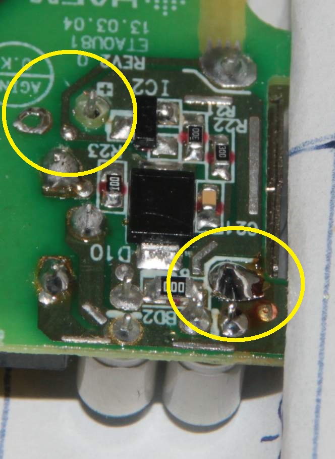
After clearing off the two lifted pads, and bending the pins towards the closest associated conductive bits (had to scrape off the soldermask from the trace going to the positive output pin), a dab of solder on each, resulted in this abomination:

Can barely even tell it's not factory-fresh, can you? Well, not everything that passes through my hands gets hopelessly mutilated, y'know... But either way, the end-result puts out about 5.09V through a USB cable with very light load on the other side. Way better than before, i'm sure you'll agree.
No comments:
Post a Comment