
The HP dock though, was about 15$, but came with a ma-HOO-sive 230W power brick, which is for another project; expect a teardown of the brick soon. Sadly the dock wouldn't fit my HP Elitebook 6930p (only the later xx40 Elitebooks), but that doesn't mean we can't take a peek under the skirts, and then resell it to make some of the money back, right?
Starting off with the HP, a pretty comprehensive complement of ins & outs - two PS/2 ports, serial and parallel ports, VGA / DVI / DisplayPort video outputs, RJ45 LAN connection, four USB 2.0 ports (two of which are on the side), line in/out, DC input and E-monitor stand connector (which, from what i've read, basically contains power button & status LED connections).


An entire fourteen T8 M2.5 machine screws removed later, and the first piece to come off is the top cover of the rear section, revealing the daughterboards and light-guides for the two status LEDs (on the sides), as well as the sliding mechanism for the spacer-blocks (in the middle).

Removing the four screws from the former enables removing of the whole top half (containing the ejection system mechanicals) in one fell swoop.

Call me weird, but there's just something really comforting / satisfying about stuff made for the industrial or enterprise segments. Very little penny-pinching and corner-cutting, because it's a longer-term commitment than the latest disposable cheapo plasticky consumer gadgets. The main lever is most likely an aluminium / aluminum alloy, and not much expense spared on the plastics either - polycarbonate-ABS blend, with 40% glass-fiber filling, apparently from Bayer.


Pretty neat layout of the electronics, at first glance. But then again, there's (also) not all that much in there.

Bottom of the board's literally barren. But then again, a two-sided load would've only added to the assembly cost, and if everything fit on the top side (and with room to spare)... Interesting though, that there's an unpopulated spot for what looks to me like a SATA connector, some QFN16-packaged chip and some passives; i guess there might(?) be versions of this with an eSATA port as well. The 8440p schematic does indeed show two sets of SATA signals going into the docking connector.

Interesting though, that there's an unpopulated spot for what looks to me like a SATA connector, some QFN16-packaged chip and some passives; i guess there might(?) be versions of this with an eSATA port as well. The 8440p schematic does indeed show two sets of SATA signals going into the docking connector. The bigger brother of this (the "Advanced Docking Station") has space for an optical drive plus an eSATA connection, so that's likely the reason.
The group of four devices connected to the huge power planes is most likely a set of P-MOSFETs, in charge of switching the power from the DC input to the appropriate pins in the docking connector. Sure enough, that's exactly what those FDMC6675BZ's are. The AS393 near those might be doing some undervoltage protection or something. Doubtful it's doing anything else, since there are no current shunts or other opamps on the board.
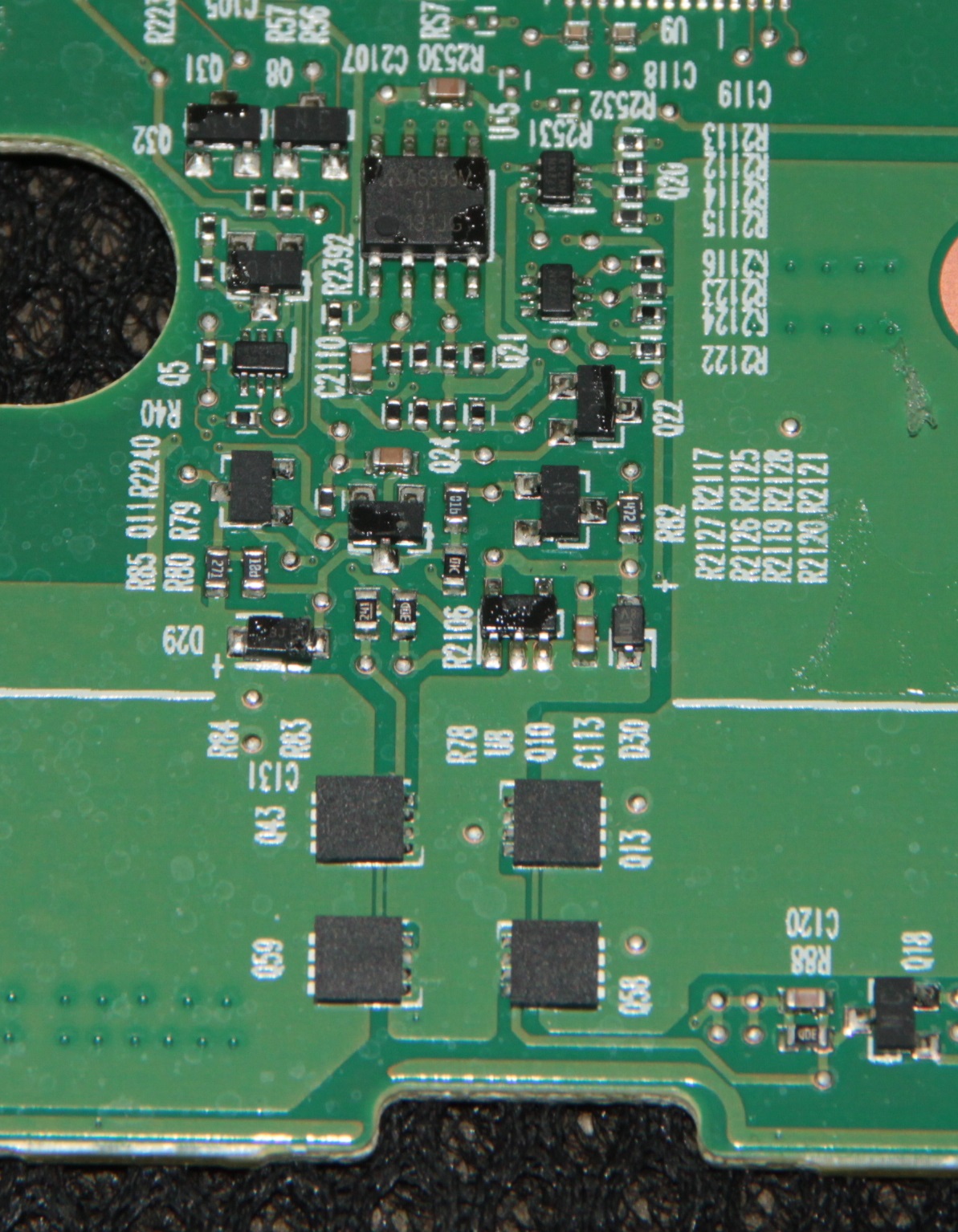
Keeping with the power circuitry, a TI TPS51117 is, most likely, handling the 5V supply going to the USB connectors, and the two silver electrolytics are likely Chemicon PSA's. The DPAK-packaged APL1085 adjustable LDO would be dropping that 5V to 3.3V, which supplies all the logic circuitry on the board. Interestingly enough, the SOT223-packaged "GH17R" is an AZ1117 5V LDO - not quite sure what that does or what it's supplying though, but it's fed from the main DC input. Might just be some 5V stand-by supply, which doesn't need much current.

Speaking of USB power, the 5V is then routed through three uP7534A (1.5A typical) load switches, and one G546A1. The data lines of said USB ports are handled by an SMSC (nowadays Microchip) USB2514B hub.

The DisplayPort output is driven by a Parade Technologies PS8121ED repeater.

The DVI output, on its separate little daughterboard, is handled by a PS8101 level shifter.

And last but not least, the ZT3243LEEA seems to be the serial port interface chip.

Right then, onto the smaller Dell PR03X.


Full-enough roster of connections here as well - no "legacy" connectors to be found, and one less USB 2.0 (the other three are on one side, along with the two 3.5mm audio jacks), but we gain two USB 3.0 ports, as well as an eSATA-USB 2.0 combo port, arguably more useful than the plain eSATA version.
15 screws later, and we're in. Unlike the HP, this time around the bottom cover comes off first. The mechanicals already look somewhat more involved.


A few more screws later, the bottom plate comes off - board's made by Compal (one of the bigger computing PCB OEM's). And this time around, we do have a two-sided load, although to be fair, we've arguably got more connections in a considerably tighter overall footprint.


This time, we do have a current-shunt in the DC input area, and the AS393 may be handling some form of protection. Probably not overcurrent though, since one half of it is connected to ground. The AP2172A is the load switch for two of the three side USB 2.0's, another one for the two USB 3.0 ports, and yet another one for the eSATA/USB 2.0 combo port, plus the AP2311 is for the third side USB 2.0.

Power section's a little bit more involved than the earlier one too - we have a Richtek RT8206L, handling both the 5V and 3.3V power rails. Nice beefy inductors, too.

Biggest chip on the board is the USB 3.0 hub, an SMSC (once again, nowadays Microchip) USB5534B.

The USB 2.0 hub is an SMSC USB2153B. The PS8330B next to it is the DisplayPort repeater.

The PS8171 is the level shifter for the DVI output.

Interestingly enough, there's actually a full-blown codec in here as well, for the audio input & output, namely an Analog Devices SSM2603.

Interestingly enough, there's also an ECE1099. Most likely it's hooked up to the SMBUS, but i can't quite figure out what the outputs might be controlling. Some sort of power-sequencing, perhaps? A bunch of the 0402 resistors on one side seem to be arranged in a "configuration jumper" type matrix, so... Your guess is as good as mine.

Other than that, a handful of MOSFETs for routing power around the board, a couple polyfuses / PPTC's protecting the various power outputs (part of the DisplayPort, DVI and VGA outputs), and that about covers it, i guess.
No comments:
Post a Comment